The Via for PCBs
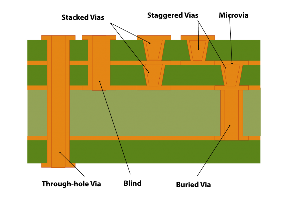 In printed circuit board design, a via consists of two pads in corresponding positions on different layers of the board, that are electrically connected by a hole through the board. The hole is made conductive by electroplating, or is lined with a tube or a rivet. High-density multilayer PCBs may have microvias: blind vias are exposed only on one side of the board, while buried vias connect internal layers without being exposed on either surface. Thermal vias carry heat away from power devices and are typically used in arrays of about a dozen.1)